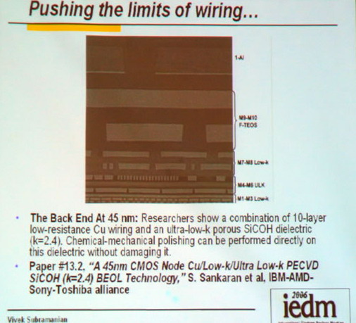
Auf dem International Electron Device Meeting (IEDM) in San Francisco haben AMD und IBM weitere Details zum gemeinsam entwickelten 45nm-Prozess bekanntgegeben.
Bei diesem Prozess soll Immersions-Lithografie, sowie ein "Ultra-Low-k"- (ULK-)Dielektrikum aus Organosilikatglas zum Einsatz kommen. Der Prozess wird bei heise online näher beschrieben.
In der Pressemitteilung werden erste Produkte auf Basis dieses Fertigungsprozesses für Mitte 2008 angekündigt.
"The continued enhancement of AMD and IBM's transistor strain techniques has enabled the continued scaling of transistor performance while overcoming industry-wide, geometry-related scaling issues associated with migrating to 45nm process technologies. In spite of the increased packing density of the 45nm generation transistors, IBM and AMD have demonstrated an 80 per cent increase in p-channel transistor drive current and a 24 per cent increase in n-channel transistor drive current compared to unstrained transistors. This achievement results in the highest CMOS performance reported to date in a 45nm process technology."


Diesen Artikel bookmarken oder senden an ...


