Samsung Electronics Begins Mass Production at New EUV Manufacturing Line
SamsungŌĆÖs EUV capacity under 7nm will triple by end of 2020
To start ship┬Łping first 7 and 6nm-based mobi┬Łle chips from V1 line in 1Q
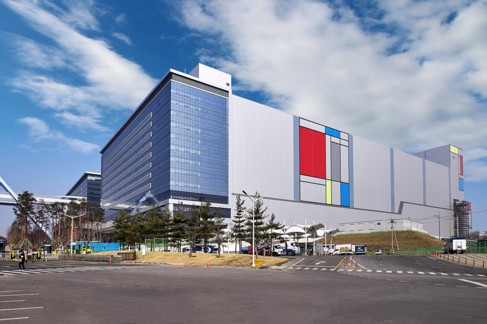
Sam┬Łsung Elec┬Łtro┬Łnics, a world lea┬Łder in advan┬Łced semi┬Łcon┬Łduc┬Łtor tech┬Łno┬Łlo┬Łgy, today announ┬Łced that its new cut┬Łting-edge semi┬Łcon┬Łduc┬Łtor fabri┬Łca┬Łti┬Łon line in Hwa┬Łse┬Łong, Korea, has begun mass production.
The faci┬Łli┬Łty, V1, is SamsungŌĆÖs first semi┬Łcon┬Łduc┬Łtor pro┬Łduc┬Łtion line dedi┬Łca┬Łted to the extre┬Łme ultra┬Łvio┬Łlet (EUV) litho┬Łgra┬Łphy tech┬Łno┬Łlo┬Łgy and pro┬Łdu┬Łces chips using pro┬Łcess node of 7 nano┬Łme┬Łter (nm) and below. The V1 line bro┬Łke ground in Febru┬Łary 2018, and began test wafer pro┬Łduc┬Łtion in the second half of 2019. Its first pro┬Łducts will be deli┬Łver┬Łed to cus┬Łto┬Łmers in the first quarter.
ŌĆ£Along with tech┬Łno┬Łlo┬Łgy lea┬Łder┬Łship and design infra┬Łstruc┬Łtu┬Łre, manu┬Łfac┬Łtu┬Łring excel┬Łlence is one of the most important ele┬Łments of the foundry busi┬Łness,ŌĆØ said Dr. ES Jung, Pre┬Łsi┬Łdent and Head of Foundry Busi┬Łness at Sam┬Łsung Elec┬Łtro┬Łnics. ŌĆ£As we ramp up pro┬Łduc┬Łtion, the V1 line will enhan┬Łce our abili┬Łty to respond to mar┬Łket demand and expand oppor┬Łtu┬Łni┬Łties to sup┬Łport our customers.ŌĆØ
The V1 line is curr┬Łent┬Łly pro┬Łdu┬Łcing sta┬Łte-of-the-art mobi┬Łle chips with 7 and 6nm pro┬Łcess tech┬Łno┬Łlo┬Łgy and will con┬Łti┬Łnue to adopt finer cir┬Łcuit┬Łry up to the 3nm pro┬Łcess node.
By the end of 2020, the cumu┬Łla┬Łti┬Łve total invest┬Łment in the V1 line will reach USD 6 bil┬Łli┬Łon in accordance with SamsungŌĆÖs plan and the total capa┬Łci┬Łty from 7nm and below pro┬Łcess node is expec┬Łted to tri┬Łple from that of 2019. Tog┬Łe┬Łther with the S3 line, the V1 line is expec┬Łted to play a pivo┬Łtal role in respon┬Łding to fast-gro┬Łwing glo┬Łbal mar┬Łket demand for sin┬Łgle-digit node foundry technologies.
As semi┬Łcon┬Łduc┬Łtor geo┬Łme┬Łtries grow smal┬Łler, the adop┬Łti┬Łon of EUV litho┬Łgra┬Łphy tech┬Łno┬Łlo┬Łgy has beco┬Łme incre┬Łasing┬Łly important, as it enables sca┬Łling down of com┬Łplex pat┬Łterns on wafers and pro┬Łvi┬Łdes an opti┬Łmal choice for next-gene┬Łra┬Łti┬Łon appli┬Łca┬Łti┬Łons such as 5G, AI, and Automotive.
With the V1 line in ope┬Łra┬Łti┬Łon, Sam┬Łsung now has a total of six foundry pro┬Łduc┬Łtion lines in South Korea and the United Sta┬Łtes, inclu┬Łding five 12-inch lines and one 8ŌĆæinch line. (see below)
* Global manufacturing sites of Samsung foundry
| Name | 6ŌĆæLine | S1-Line | S2-Line | S3-Line | S4-Line | V1-Line |
| Nodes | 180~65nm | 65~8nm | 65~11nm | 10nm~ | 65nm~ | 7nm~ |
| Loca┬Łti┬Łon | Gihe┬Łung, Korea | Aus┬Łtin, USA | Hwa┬Łse┬Łong, Korea | |||
| Wafer Size | 8ŌĆæinch | 12-inch | ||||