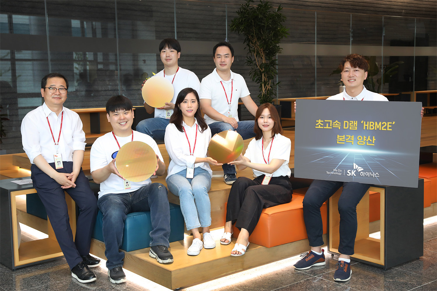
SK Hynix Starts Mass-Production of High-Speed DRAM, ŌĆ£HBM2EŌĆØ
SEOUL, South Korea, July 1, 2020 ŌĆö SK hynix Inc. (or ŌĆśthe Com┬Łpa┬Łny,ŌĆÖ www.skhynix.com) announ┬Łced that it has star┬Łted the full-sca┬Łle mass-pro┬Łduc┬Łtion of high-speed DRAM, ŌĆśHBM2EŌĆÖ, only ten months after the Com┬Łpa┬Łny announ┬Łced the deve┬Łlo┬Łp┬Łment of the new pro┬Łduct in August last year.
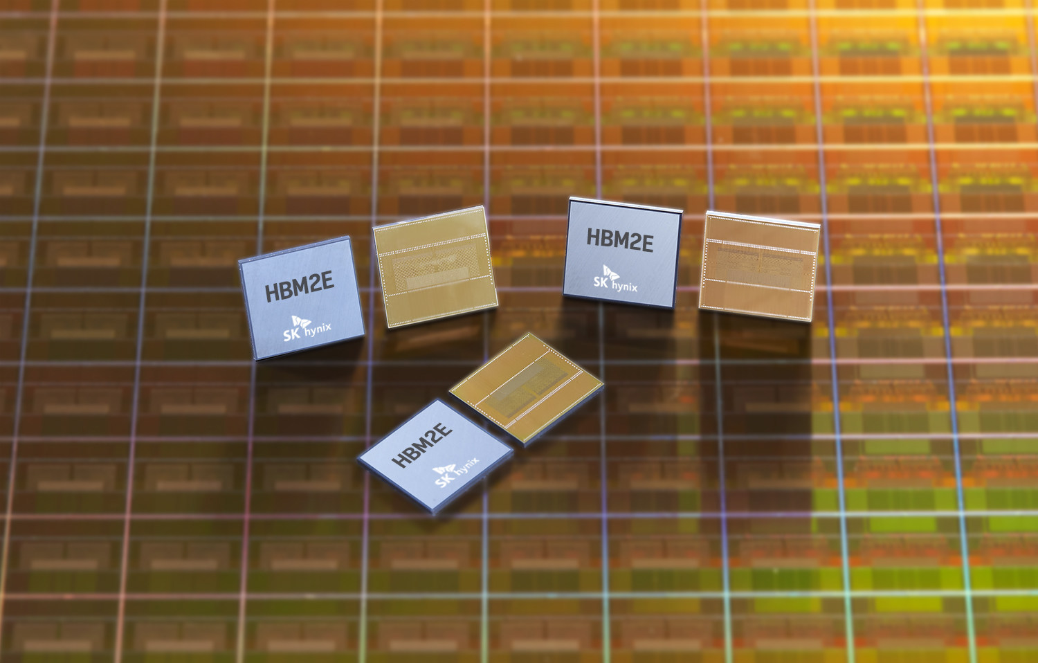
SK hynixŌĆÖs HBM2E sup┬Łports over 460GB (Giga┬Łbyte) per second with 1,024 I/Os (Inputs/Outputs) based on the 3.6Gbps (giga┬Łbits-per-second) speed per┬Łfor┬Łmance per pin. It is the fas┬Łtest DRAM solu┬Łti┬Łon in the indus┬Łtry, being able to trans┬Łmit 124 FHD (full-HD) movies (3.7GB each) per second. The den┬Łsi┬Łty is 16GB by ver┬Łti┬Łcal┬Łly stack┬Łing eight 16Gb chips through TSV (Through Sili┬Łcon Via) tech┬Łno┬Łlo┬Łgy, and it is more than dou┬Łbled from the pre┬Łvious gene┬Łra┬Łti┬Łon (HBM2).
HBM2E boasts high-speed, high-capa┬Łci┬Łty, and low-power cha┬Łrac┬Łte┬Łristics; it is an opti┬Łmal memo┬Łry solu┬Łti┬Łon for the next-gene┬Łra┬Łti┬Łon AI (Arti┬Łfi┬Łci┬Łal Intel┬Łli┬Łgence) sys┬Łtems inclu┬Łding Deep Lear┬Łning Acce┬Łle┬Łra┬Łtor and High-Per┬Łfor┬Łmance Com┬Łpu┬Łting, which all requi┬Łre high-level com┬Łpu┬Łting per┬Łfor┬Łmance. Fur┬Łther┬Łmo┬Łre, it is expec┬Łted to be appli┬Łed to the Exas┬Łca┬Łle super┬Łcom┬Łpu┬Łter ŌĆō a high-per┬Łfor┬Łmance com┬Łpu┬Łting sys┬Łtem which can per┬Łform cal┬Łcu┬Łla┬Łti┬Łons a quin┬Łtil┬Łli┬Łon times per second ŌĆō that will lead the rese┬Łarch of next-gene┬Łra┬Łti┬Łon basic and appli┬Łed sci┬Łence, such as cli┬Łma┬Łte chan┬Łges, bio-medics, and space exploration.
ŌĆ£SK hynix has been in the fore┬Łfront of tech┬Łno┬Łlo┬Łgy inno┬Łva┬Łti┬Łon that con┬Łtri┬Łbu┬Łtes to human civi┬Łliza┬Łti┬Łon with achie┬Łve┬Łments inclu┬Łding the worldŌĆÖs first deve┬Łlo┬Łp┬Łment of HBM pro┬Łducts,ŌĆØ said Jongho┬Łon Oh, Exe┬Łcu┬Łti┬Łve Vice Pre┬Łsi┬Łdent and Chief Mar┬Łke┬Łting Offi┬Łcer (CMO) at SK hynix. ŌĆ£With the full-sca┬Łle mass-pro┬Łduc┬Łtion of HBM2E, we will con┬Łti┬Łnue to streng┬Łthen our pre┬Łsence in the pre┬Łmi┬Łum memo┬Łry mar┬Łket and lead the fourth indus┬Łtri┬Łal revolution.ŌĆØ
Anno┬Łta┬Łti┬Łon
- HBM (High Band┬Łwidth Memo┬Łry)
- High per┬Łfor┬Łmance, high band┬Łwidth memo┬Łry pro┬Łducts that adopt TSV tech┬Łno┬Łlo┬Łgy to dra┬Łma┬Łti┬Łcal┬Łly acce┬Łle┬Łra┬Łte data pro┬Łces┬Łsing speed over tra┬Łdi┬Łtio┬Łnal DRAMs. - TSV (Through Sili┬Łcon Via)
- An inter┬Łcon┬Łnec┬Łting tech┬Łno┬Łlo┬Łgy that con┬Łnects the upper and lower chips through thou┬Łsands of fine holes on DRAM chip.
- Deli┬Łvers data, com┬Łmands, and curr┬Łents through column-shaped paths that pene┬Łtra┬Łte the enti┬Łre sili┬Łcon wafer thic┬Łk┬Łness after stack┬Łing mul┬Łti┬Łple DRAM chips on the buf┬Łfer chip.
- Up to 30% decrease in size and up to 50% decrease in power con┬Łsump┬Łti┬Łon over exis┬Łting pack┬Ła┬Łging methods. - Stan┬Łdards for data pro┬Łcess speed con┬Łver┬Łsi┬Łon
- 1GB = 8Gb
- 3.6Gbps per pin with 1024 data I/Os (Inputs/Outputs) = 3686.4Gbps
- 3686.4Gbps / 8 = 460.8GB/s (Gb -> GB conversion)
About SK hynix Inc.
SK hynix Inc., head┬Łquar┬Łte┬Łred in Korea, is the worldŌĆÖs top tier semi┬Łcon┬Łduc┬Łtor sup┬Łpli┬Łer offe┬Łring Dyna┬Łmic Ran┬Łdom Access Memo┬Łry chips (ŌĆ£DRAMŌĆØ), flash memo┬Łry chips (ŌĆ£NAND flashŌĆØ) and CMOS Image Sen┬Łsors (ŌĆ£CISŌĆØ) for a wide ran┬Łge of distin┬Łgu┬Łis┬Łhed cus┬Łto┬Łmers glo┬Łbal┬Łly. The CompanyŌĆÖs shares are traded on the Korea Exch┬Łan┬Łge, and the Glo┬Łbal Depo┬Łsi┬Łto┬Łry shares are lis┬Łted on the Luxem┬Łburg Stock Exch┬Łan┬Łge. Fur┬Łther infor┬Łma┬Łti┬Łon about SK hynix is available at www.skhynix.com, news.skhynix.com.